Nanostencil
patterning of In and Sn on atomically clean Si(001)
N To, S
Dobrin and
J Nogami
Materials
Science and Engineering, University of Toronto
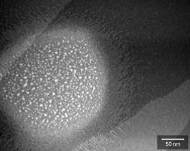 A self-aligning
nanostencil mask was used to pattern circular features of tin and indium over an
atomically clean Si(001)
A self-aligning
nanostencil mask was used to pattern circular features of tin and indium over an
atomically clean Si(001) 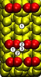 substrate. The
shadow mask limits material to deposit only where the membrane is open, leaving
adjacent clean surfaces for material to diffuse. STM is used to study the
surface diffusion of these metals in UHV. The diffusion of tin is found to be
relatively limited in comparison with indium, and remains so even at increasing
coverage. Indium forms unstable 3D islands that dissolve over time and
contribute to the spreading of a single layer thick film on the surrounding
clean surface. The difference in behaviour between the two metals can be
attributed to the difference in activation energy for diffusion of atoms on top
of the first atomic layer of metal.
substrate. The
shadow mask limits material to deposit only where the membrane is open, leaving
adjacent clean surfaces for material to diffuse. STM is used to study the
surface diffusion of these metals in UHV. The diffusion of tin is found to be
relatively limited in comparison with indium, and remains so even at increasing
coverage. Indium forms unstable 3D islands that dissolve over time and
contribute to the spreading of a single layer thick film on the surrounding
clean surface. The difference in behaviour between the two metals can be
attributed to the difference in activation energy for diffusion of atoms on top
of the first atomic layer of metal.
Density Functional
Theory (DFT) calculations were used to determine the activation barrier for a Sn or In atom traveling over
occupied 2 × 2 reconstructed metal surfaces. Equilibrium positions are shown as
1,1’ and 32. Transition states are labeled 2 and 2’.
The calculated Sn and In
atoms diffusion along and across the direction of the underlying Si dimer rows
are listed in following table.
|
|
Activation
barrier |
|
|
Direction of
the diffusion: |
Sn |
In |
|
along
dimer row |
0.6 eV |
0.2 eV |
|
across
dimer row |
1.0 eV |
0.4 eV |
Presented at: the 22nd Canadian Conference on Surfaces, 13-16 May 2011, Simon Fraser University
Burnaby, British Columbia, s“Nanostencil patterning of In and Sn on atomically clean Si(001)”, N. To, S. Dobrin, J. Nogami